Exploring the Limits of Resolution — How Scientists Use TEM to See Atoms
Wiki Article
If you’ve ever wondered how far we can go when zooming into the tiniest building blocks of matter, you’re not alone. From seeing cells and bacteria to observing atoms themselves — microscopes have evolved far beyond what our eyes can imagine.
So, what’s the most powerful microscope in the world today?
The answer is: the Transmission Electron Microscope (TEM) — capable of magnifying up to 50 million times and even resolving individual atoms.
Let’s explore how it works, how it compares to other microscopes, and why it stands at the top of modern science.
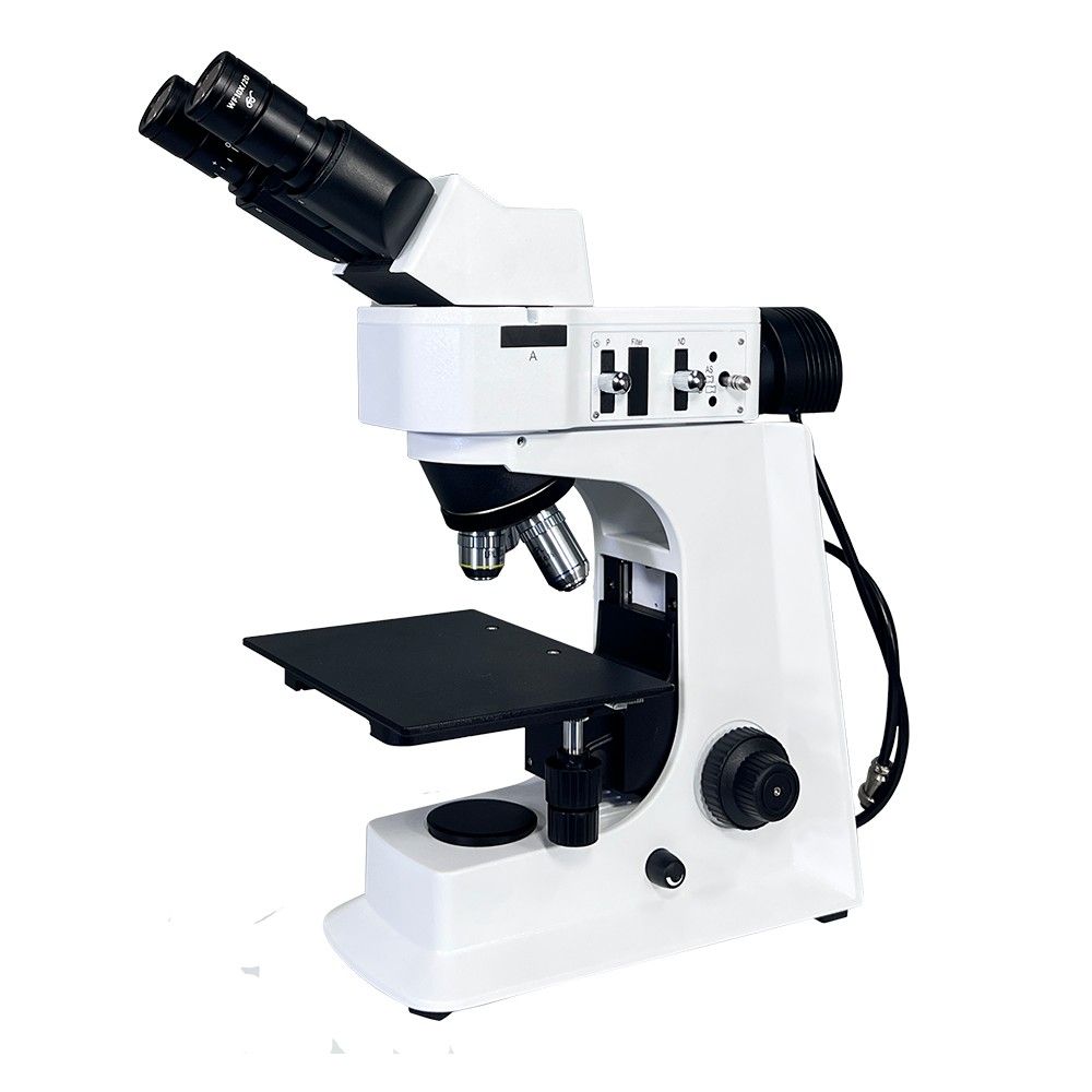 SCOPE MIT200 Metallurgical Microscope
The Evolution of “Powerful” Microscopes
To understand what makes a microscope powerful, we need to look at two things:
- Magnification:how much the image is enlarged.
- Resolution:how close two points can be and still be distinguished as separate.
It’s not just about zooming in — it’s about how clearly we can see the tiniest structures.
Here’s a quick look at how microscope technology evolved:
Type | Maximum Magnification | Resolution | Typical Use |
Optical Microscope | 1000× – 2000× | ~200 nm | Cells, bacteria, metals |
Scanning Electron Microscope (SEM) | 100,000× – 1,000,000× | ~1 nm | Surface structures |
Transmission Electron Microscope (TEM) | 10,000,000× – 50,000,000× | <0.1 nm | Atomic-level imaging |
Transmission Electron Microscope (TEM) — The Champion
TEMs are the most powerful microscopes in existence.
Instead of light, they use a beam of high-energy electrons that pass through an ultra-thin specimen. Because electrons have a much shorter wavelength than visible light, they can resolve details at the atomic level — smaller than one-billionth of a meter.
Key facts about TEM:
- Magnification:Up to 50 million×
- Resolution:About 05 nm (50 picometers)
- Can visualize:Atoms, crystal lattice defects, nanoparticles, viruses
Applications include:
- Nanotechnology research
- Semiconductor materials
- Crystallography
- Virus and cellular ultrastructure studies
In short — if you want to see atoms, TEM is your go-to instrument.
Other Extremely Powerful Microscopes
While TEM is the reigning champion, a few other contenders are worth mentioning:
Scanning Transmission Electron Microscope (STEM)
Combines the principles of SEM and TEM — scans a focused electron beam over a thin sample for high-resolution 3D atomic mapping.
Used in material science and advanced nanotech.
Scanning Electron Microscope (SEM)
Provides detailed surface images with magnifications up to 1 million×.
It’s widely used in metallurgy, forensics, and microelectronics — though it doesn’t reach atomic resolution.
Atomic Force Microscope (AFM)
Instead of electrons or light, AFM uses a nano-scale probe to feel the surface atoms.
It can measure atomic forces and build 3D topographic maps with sub-nanometer precision.
Scanning Tunneling Microscope (STM)
STM works on the principle of quantum tunneling — allowing it to image and even manipulate individual atoms.
Some call it “the microscope that sees atoms in action.”
Why We Don’t Always Use the “Most Powerful” Microscope
Despite their power, electron and scanning probe microscopes come with limitations:
Factor | Limitation |
Sample prep | Requires ultra-thin, vacuum-compatible specimens |
Cost | Millions of dollars + specialized lab setup |
Operation | Needs highly trained personnel |
Speed | Slower imaging and analysis |
Environment | Sensitive to vibration and magnetic fields |
That’s why for everyday use — from biology labs to metal inspections — optical and digital microscopes are still the most practical choice.
The Bottom Line
So, what’s the most powerful type of microscope?
The Transmission Electron Microscope (TEM) — capable of resolving individual atoms, reaching up to 50 million× magnification, and unlocking the deepest secrets of matter.
But remember:
“Powerful” doesn’t always mean “useful.”
Each microscope serves its own purpose — whether you’re studying cells, alloys, or atoms.
Microscope Type | Magnification Range | Resolution | Key Advantage |
Optical | 40× – 2000× | 200 nm | Simple, real-color imaging |
SEM | 1,000× – 1,000,000× | 1 nm | Surface detail and texture |
TEM | Up to 50,000,000× | <0.1 nm | Atomic-scale imaging |
AFM | Up to 1,000,000× | <0.1 nm | 3D surface mapping |
STM | Up to 100,000,000× | Atomic level | Visualizes and manipulates atoms |
Final Thoughts
Microscopes have come a long way — from seeing cells to seeing atoms.
If your goal is to understand how materials behave at their most fundamental level, the Transmission Electron Microscope is the most powerful tool ever built by science.
But if your daily work involves biological samples, metals, or materials inspection, even a modest optical or digital microscope can deliver everything you need — clarity, efficiency, and practical usability.
Report this wiki page